| Back |
|---|
Following a couple of articles in the VARC Newsletter earlier this year on Klystrons and Magnetrons, I have been asked to explain in more detail the interaction between E-M waves and the electron beam. This article will concentrate on the klystron amplifier and a similar device, the Travelling Wave Tube.
Recap
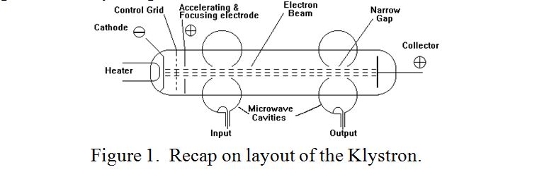
In a klystron amplifier, a weak signal in the microwave resonant input cavity causes velocity modulation of the electron stream. This results in the faster electrons in the beam catching up with those in front and the slower electrons falling into those behind. Thus “bunching” occurs which increases with distance travelled as the electrons travel along the field free drift space beyond the input cavity. Hence the density or concentration of electrons becomes periodic along the electron beam with maxima and minima. To recap on the layout of a typical klystron amplifier, the relative positions of the input cavity, output cavity and electron beam are shown diagrammatically in figure 1.
This periodicity in electron density would be interpreted by an electron collecting anode as an amplified periodic current, (compared to the weak RF input). (In actual fact, the output RF is not taken from the anode as in a thermionic valve, but from another resonant cavity further along the electron beam, but this does not affect the validity of the description). The bunching, small at first, becomes more pronounced as the electrons proceed along the beam as the process of catching up and falling behind takes effect. The region in which they do this is known as the “Drift Space” and this normally contains several “alternations” of bunching, i.e. regions of high and low density. You might think that this process is almost “amplification without limit” needing no further human intervention; all you have to do is make the drift space long, (in the case of a klystron), and put a suitable resonant cavity at the end of it to collect the much amplified RF signal. Unfortunately, this is not so as shown below.
Practice
RF signals are “sine waves”, either voltages and currents in a wire or waves in space. An input cavity, (or Rhumbatron as it is sometimes called), modulates the velocity of an electron beam by means of its electric field being in the same direction as the beam. Moreover, it modulates the velocity of the beam in a sine wave manner. However, the bunching process caused by velocity modulation is not linear, resulting in the density of the electron beam only being of sine wave form for very low modulation depths. The result is that the electron density profile becomes less and less sine wave like as the electrons travel, and thus contains less and less of the fundamental frequency and more and more harmonics. A rough impression of the density profile of the electron beam as it passes an observer at four points in the drift space is shown in figure 2.
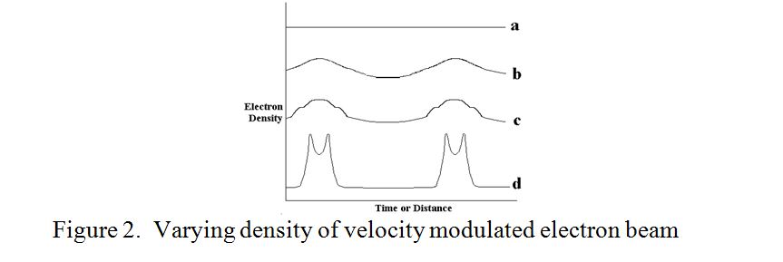
‘a’ represents the constant density, velocity modulated electron beam before significant bunching has occurred. ‘b’ represents a small degree of bunching, and is still of roughly of sine wave form. ‘c’ shows considerable distortion, with the development of “shoulders” on the bunch, and ‘d’ represents the maximum distortion which can occur. At a point further down the electron beam, the “pulse like” shape disperses into a more uniform profile again. The peaks in lines ‘b’ and ‘c’ are of course 360 degrees of phase apart and the double peaks at maximum distortion, ‘d’ are 86 degrees of phase apart. Another effect which occurs in high power klystrons is the spreading of the electron bunches due to the mutual repulsion of electrons. The net result of a long drift space is that there are more harmonics in the profile of the beam than fundamental frequency. These result in a practical limit to both the maximum power and the gain which can be achieved by simple two cavity klystrons.
However, all is not lost. By inserting one or more dummy resonant cavities, (i.e. cavities from which power is neither input nor output), which interact with the electron beam, the misshapen beam profile may be reformed by “shepherding” electrons in the wrong place back into something like a sine wave profile. The net result is that modern multi-cavity klystrons can have efficiencies, (i.e. RF power out divided by DC power in), of several 10s of percent, and are frequently used in space satellites for sending signals back to earth.
Klystrons can also be used in reverse. By feeding substantial amounts of RF power into the resonant cavities along the beam, the electrons, or indeed other ionised particles in the beam, can be accelerated to near the speed of light as is required for nuclear physics “atom smashing” experiments. This process has been likened to a surfer riding an incoming wave.
The Travelling Wave Tube
An important variant of the multi-cavity klystron is the travelling wave tube, (TWT). In this, electron acceleration and deceleration to form bunches is a continuous process rather than in a single step process as performed by the input cavity of a klystron amplifier. It is again achieved by subjecting the electrons to a longitudinal electric field, (i.e. aligned with the electron beam), which is produced in a “structure” by the input signal, (as described in the next paragraph). Initially the weak input signal is caused to velocity modulate the electron beam, but when the bunching becomes large, as it does naturally with time and distance, the bunched electrons within the structure feed back energy into the travelling wave. The surfer riding a sea wave is again relevant. Just as a surfer, extracting energy from a sea wave, has to keep up with the wave, so does the signal have to keep pace with the electron beam.
However, for modest valve voltages, (a few hundred volts), electrons travel at only a small fraction of the speed of light So if a group of electrons is to “ride an electro-magnetic wave” like a surfer, and the electrons cannot be made to travel at Mega-volt speeds, the wave has to be slowed down. Producing a “slow wave structure ” and a longitudinal electric field for the input signal can be performed in a single step by a suitable spiral or helix of wire.
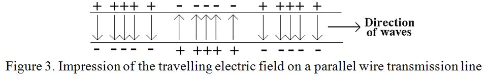
Electric field can be imagined as the “force field” which exists between opposite electric charges. i.e. the field “flows” from positive to negative fixed charges. If a negative charge were to be placed between these fixed charges it would be pushed from the negative charge towards the charge positive. An electrical signal on a transmission line, can be thought of as a succession of alternate charges, (positive and negative), with accompanying electric fields travelling along the transmission line, (assumed to be in a vacuum), at the speed of light. A simple representation of a snapshot in time of this situation is shown in figure 3.
If the helix is so dimensioned that the signal, travelling at the speed of light along the wire forming the helix, has advanced 180 degree in phase between adjacent turns, then identical points on adjacent turns will be in anti-phase. Some of the electric field lines between adjacent turns of the helix will have a longitudinal direction coinciding with that of the electron beam as indicated by the arrow in figure 4.
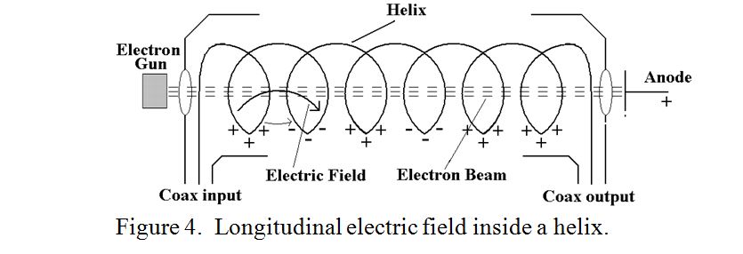
It is these longitudinal field lines which accelerate or decelerate the electrons causing velocity modulation which causes them to bunch. Rather like the intermediate cavities of a multi-klystron amplifier, the electrons are shepherded into and kept in a sine wave form. The amplitude of the bunching grows with distance, as does the electric field caused by the bunching, resulting in the signal current growing in the helical wire until it is output at the far end of the tube by a similar transition to that at the input end. Several other mechanisms are employed to keep the process stable and to enable the TWT to amplify over a reasonable band width but these are the basic mechanisms.
PRAECEPTOR
| Back |
|---|