AB INITIO
| Back |
|---|
I’m afraid this article is a bit technical, but this really can’t be avoided if you are going to get any inkling of how a semi-conductor diode works.
The word “diode” means any “active” two electrode device used in electronics There are two main sorts, Thermionic and Semi-conductor. The former was dealt with in a previous article. Of the latter there are many different sorts such as Gunn, impatt, light emitting, photo, pin, rectifier, Schottky, trapat, tunnel, varactor, Zener etc. Semi-conductor diodes can be used as oscillators and light or IR emitters, as voltage controllable resistors or capacitors, as rectifiers and signal detectors, or as voltage references. However, when the word “diode” is unprefixed by any other adjective, it usually refers to a rectifier and that is the main theme of this article as it is used to explain the workings of the “p-n junction”.
The first application of semi-conductor diodes as rectifiers was in the “Crystal Set” of the early 1900s to the mid 1920s. This usually employed a crystal of Galena, (Lead sulphide), and a metallic point contact as a rectifier, or “detector” of radio signals. Other materials were also employed of which the most popular was carborundum and a steel point. These were considerably more sensitive than the thermionic diode, (which was also under development at this time), although the thermionic diode was preferred in vibration and maritime environments as it was more stable and reliable.
The “crystal and cat’s whisker” effect was discovered at about the same time as the “coherer”, but it was not until 50 years after its discovery that its operating mechanisms were properly understood. In fact understanding it had to wait until modern quantum theory had been developed, with its restrictions on allowable electron energy, energy bands, band gaps and forbidden zones. Explaining its operation without resort to these is difficult and has to rely heavily on analogy, but the following is a rough attempt.
All matter consists of atoms, each of which comprises a nucleus with a fixed number of positive charges, (depending on the chemical element), surrounded by an equal number of negative electrons in more or less fixed orbits. A good analogy for a single atom is a sun surrounded by planets in orbit. In the presence of neighbouring atoms, the outer, (or “valence”) electrons may share their orbits with the neighbouring atoms, thus binding them together. In an insulator, no electron can be easily pulled out of its orbit, whether from its parent atom or its compound with a neighbouring atom. In a conductor, one or more of the outer electrons is free to “float” and share with any other atom. (At this point, we have to introduce the idea that there are many different conduction mechanisms appropriate to solids, liquids and gasses. We shall deal with only two of them applicable to solids: conduction by electrons and conduction by “holes”).
In crystalline carbon, (diamond), Silicon, Germanium, and some other substances, each atom has 4 outer electrons available for sharing which it does with 4 immediate neighbours, leaving none free to float or roam. The pure “intrinsic” material is therefore a moderately good insulator, particularly at low temperature. If however, a small amount of a foreign substance, such as phosphorus, arsenic or antimony, having 5 outer electrons is alloyed with silicon, (say), its fifth electron has nothing to bond to and is free to roam, making the alloy a (not very good) conductor. If however a foreign substance such as boron, aluminium, gallium, or indium, having 3 outer electrons is alloyed with the silicon, this leaves a “hole” between it and its neighbouring Silicon atom which a neighbouring valence electron may pop into, thus leaving a hole behind it, so this alloy also becomes a moderate conductor. (The absence of an electron where one should be looks like a positive charge). Both these alloys are “semi-conductors”. The former is known as “n-type” and the latter as “p-type”, but they have rather different conduction mechanisms. Free electrons can go anywhere but holes can only exchange places.
What happens at the junction of an n-type and a p-type semi-conductor with their different conduction mechanisms? In the absence of any applied voltage to the free ends of a piece of “p-type-pn junction-n-type” material, and at normal temperatures, all the atoms, electrons and holes are in a state of thermal agitation. The electrons and holes in particular are constantly jogging about and exchanging positions whilst the body of the material remains electrically neutral. The result of this is that some electrons from the n-type material diffuse a short way into the p-type material and vice-versa. In this junction region of the two types of material, the electrons neutralise the nearby positive holes, and similarly holes diffusing from the p-type material into the n-type neutralise some of the electrons there. Thus, the n-type material acquires a small positive charge, (because it has lost some electrons), and the p-type material similarly acquires a small negative charge. The region at the interface, (where the electrons and holes have neutralised each other), is known as the “depletion region”, and for the moment anyway, it has no charge carriers of either polarity. (The actual mechanism is a little more complicated than this, but this will serve for this simplified explanation). The depletion layer behaves like an insulating layer although it is not one, because it will readily conduct charges of either polarity if they can be injected into it, by for example, absorbing a photon which creates a charge pair, (electron and hole). (This is the mechanism of the photo-diode). An analogy of the depletion region is the vacuum inside a thermionic device which remains a perfect insulator but will conduct if electrons are injected into it. See a representation of the semi conductor junction in figure 1.
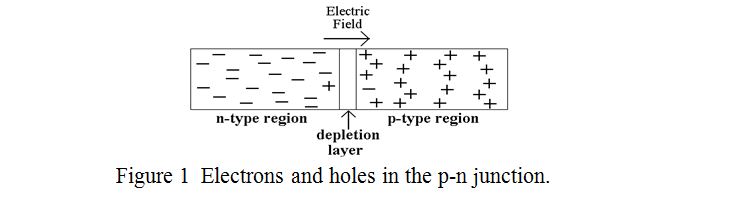
(Note that in the diagram, the –s and +s indicate only the free roaming electrons and holes. The ionised atoms from which they came are not shown).
Because the n-type side of the “p-n junction” is now positive and the p-type side is negative, a small electric field exists from the n-type to the p-type materials across the depletion region. The potential difference across this region is about half to one volt, (depending on the material). This electric field opposes any further diffusion by pulling back any excess diffused charges and so keeps a balance between thermal diffusion and electric field. If now an external voltage is applied to the remote ends of the bar of “n-type, depletion layer and p-type” material, what happens depends on which way round the voltage is applied. If the n-type end is connected to the positive part of the circuit and the p-type to the negative, the internal field is enhanced and the available free electrons and holes are pulled further apart, i.e. the depletion region widens and becomes a more effective insulator, so no current flows. (Incidentally, the moving apart of the conducting regions, of n-type and p-type material, is equivalent to moving apart the plates of a capacitor, and this mechanism forms the basis of the “Varactor diode”).
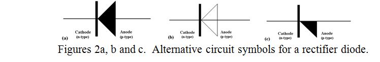
If the external supply is connected the other way round, i.e. with the n-type end connected to the negative part of the circuit and the p-type end connected to the positive part of the circuit, then, when the applied potential difference across the junction exceeds that due to the internal field, the depletion region shrinks and vanishes. The electrons can then move towards the positive end of the bar and the holes can move towards the negative end. Positive charges moving in the direction of the applied voltage and negative charges moving in the other direction constitutes a current. Where the electrons and holes meet at the junction they annihilate each other. A useful analogy, (and many electro-magnetic phenomena are best explained by analogy), is that of red coated, (positive), soldiers advancing one way and blue coated, (negative), soldiers advancing the other way and eliminating each other at the front line, (the junction). This occurs when both armies are ordered to advance. When connected the other way round, both colours of troops are ordered to retreat from the front line and there is no elimination of soldiers, (charges). Again, positive charges moving in the direction of the applied voltage and negative charges moving in the other direction constitutes a current. Hence, the semiconductor diode only allows current to flow in one direction. It is a rectifier. The usual circuit symbols for a semiconductor rectifier diode are shown in figures 2a, 2b and 2c where the direction of positive current flow is indicated by the direction of the arrows.
It is interesting to note that the very earliest semiconductor diode, the “crystal and cat’s whisker”, actually employed some of the advanced principles used in the most modern high performance semiconductors, i.e. a metal-semiconductor junction known as a “Schottky junction”, and a compound of two elements as its semiconductor. Description of the working of these however is beyond the scope of this article.
| Back |
|---|
PRAECEPTOR.